Wednesday, 31 July 2013
Friday, 19 July 2013
Monday, 8 July 2013
How to use DCM(PLL) as frequency multiplier on FPGA
Phase Locked Loop (PLL)
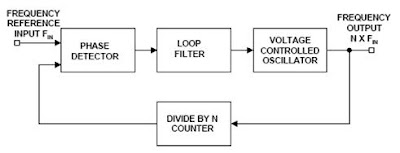
can be used as frequency multiplier. Figure3.1 shows how PLL works as frequency
multiplier.
Phase Locked Loop (PLL) circuits are
used for frequency control. They can be configured as frequency multipliers,
demodulators, tracking generators or clock recovery circuits. Each of these
applications demands different characteristics but they all use the same basic
circuit concept. Figure 3.1 contains a block diagram of a basic PLL frequency
multiplier. The operation of this circuit is typical of all phase locked loops.
It is basically a feedback control system that controls the phase of a voltage
controlled oscillator (VCO). The input signal is applied to one input of a
phase detector. The other input is connected to the output of a divide by N
counter. Normally the frequencies of both signals will be nearly the same. The
output of the phase detector is a voltage proportional to the phase difference
between the two inputs. This signal is applied to the loop filter. It is the
loop filter that determines the dynamic characteristics of the PLL. The
filtered signal controls the VCO. Note that the output of the VCO is at a frequency
that is N times the input supplied to the frequency reference input. This
output signal is sent back to the phase detector via the divide by N counter.
Normally the loop filter is designed to match the characteristics required by
the application of the PLL. If the PLL is to acquire and track a signal the
bandwidth of the loop filter will be greater than if it expects a fixed input
frequency. The frequency range which the PLL will accept and lock on is called
the capture range. Once the PLL is locked and tracking a signal the range of
frequencies that the PLL will follow is called the tracking range. Generally
the tracking range is larger than the capture range.
The
Xilinx Spartan-3 and VirtexIIPro series FPGA are all equipped with DCM (Digital
Clock Manager) modules which can precisely control the system clock [8]. There
are four DCMs available in spartan-3 kit which is considered as target device
for this project. There are three ways to use the DCM. First, calling DCM as a component is through HDL.
Second is through schematic i.e. taking as a symbol and assign ports for
required pins, then create user symbol to use in schematic. Third is through
XILINX clocking wizard from IP (Coregen & Architecture wizard). Third
one is the easiest way which is explained in subsection
Procedure
to Use DCM
Step1: Double-click Create New Source
– Select IP (COREGen & Architecture
Wizard), and click Next
The Architecture Wizard Contains Several Wizards as shown in figure 3.2.
Figure
3.2 Selecting a DCM from clocking wizard
Step2:
The Clocking Wizard helps you define the DCM. In main window
– Select pins
– Specify
• Reference source
• Clock frequency
• Phase shift
Figure 3.3 General setup wizard for DCM as a
frequency multiplier
Step3: Specify the
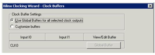
Types of Clock Buffers
Connect clock
buffers (BUFG, BUFGMUX) to the selected output pins of the DCM
The DCM will appear in source window and ready to
use as a component. It can also be used in schematic by making it as a user
symbol through ‘design utilities’ option as shown in Figure3.5. Figure 3.6
shows behavioral simulation of DCM as frequency multiplier.
Figure 3.5 DCM used as a symbol in schematic design
entry
Figure
3.6 Behavioral simulation of frequency multiplier
Friday, 28 June 2013
SCHEMATIC DESIGN ENTRY and FLOORPLANNING using Xilinx
SCHEMATIC DESIGN ENTRY
The
Xilinx Integrated Software Environment (ISE) allows users to design circuits
for Xilinx FPGA’s and CPLD’s. It involves the use of Project Navigator, a user
interface that helps user to manage the entire design process including design
entry, simulation, synthesis, implementation and finally downloading the design
onto an FPGA or CPLD.
1. Start ISE from the Start menu by
selecting Start -> Programs -> Xilinx ISE 9.2 -> Project Navigator.
The ISE Project Navigator opens. The Project Navigator manages
the sources and processes in ISE project.
2. The next step is to create a new ISE
project. To create a new project for this tutorial:
Ø Select
File -> New Project. The New Project Wizard appears as shown in
Figure 2.2
Ø First,
enter a location (directory path) for the new project.
Ø Type
fadd (for example) in
the Project Name field. After typing fadd in the Project Name field, a counter
subdirectory is created automatically in the directory path selected.
Ø Select
Schematic in the Top-Level Source Type list, indicating that the
top-level file in project will be a schematic rather than HDL, EDIF or NGC/NGO.
Click Next to go to the Device Properties window.
3. In the Device Properties window,
select Target device, Simulator tool, Synthesis tool and Hardware language
which is used to design code.
4. Click Next three times and
reach the Project Summary window. This window gives an overview of
project created so far. Click on Finish and the project is created.
Verify that the project name is fadd.ise (shown as the last component
in the title bar of the Project Navigator). You can also verify by going to the
location where you created the project and double-clicking on the folder named fadd.
5. Create a top level schematic for your
design. In the Sources window, right click on
xc3s400-4pq208 and
select New Source. A New Source Wizard window appears as shown in
Figure 2.3. Select Schematic and enter fadd under file
name. Make sure the “Add to project” checkbox is checked.
Figure 2.3 Creation
of a schematic source file
6. Click Next two times followed
by Finish to create the fadd.sch file under the project
folder. Figure 2.4 shows the final layout of the project after the source file
is created. If the schematic is not visible, click on the “fadd.sch” tab at the
bottom of the main design window to see the schematic.
Ø Select
the required components from symbols by
specifying proper category in source window.
Ø Drag
and drop the component symbols.
Ø Assign
ports and complete the circuit using wire.
Ø Check
errors and warnings. Clearing those errors is must.
Ø Follow
the standard procedure for simulation, synthesis and implementation
FLOORPLANNING
Introduction
Floorplanning
is the process of:
Ø Choosing
the best grouping and connectivity of logic in a design, and
Ø Manually
placing blocks of logic in an FPGA device.
The
goals of floorplanning are to:
Ø Increase
density, routability, or performance.
Ø Reduce
route delays for selected logic by suggesting a better placement.
Floorplanning has become necessary as
designers create ever-more complex designs for ever-larger FPGA devices.
Implementation software has improved to meet these complexities. On some
designs, you can guide the implementation software by means of a floorplan to:
Ø Higher
system clock frequency
Ø Shorter
implementation run times
Ø Greater
consistency in timing
Ø In
some cases, all of these benefits together
Benefits
of Floorplanning
A good floorplan can:
Ø Improve
performance.
Ø Enable
a placed and routed design to meet timing.
Xilinx recommends floorplanning when a
design:
Ø Does
not meet timing consistently, or
Ø Has
never met timing.
When
to Floorplan
When to floorplan varies greatly among
design teams. Design teams may floorplan:
Ø Before
the first iteration through place and route.
Ø When
a problem is identified before floorplanning.
Ø When
a design does not consistently meet the setup timing constraint.
Floorplanning
Considerations
Ø Floorplanning
is often an iterative process. The first pass at a floorplan may address issues
in one section of the design, only to reveal that a different section is failing.
Ø Floorplanning can hurt timing as well as
improve it.
This
is especially true when it is not clear what needs to be floorplanned, and
where the design needs to be placed.
Ø Multiple
trials and notes about the design can help you create a working floorplan.
Floorplanner
The
Floorplanner is a graphical placement tool that gives you control over placing
a design into a target FPGA using a “drag and drop” paradigm with the mouse
pointer.
The Floorplanner displays a hierarchical
representation of the design in the Design Hierarchy window using hierarchy
structure lines and colors to distinguish the different hierarchical levels.
The Floorplan window displays the floorplan of the target device into which you
place logic from the hierarchy. The following figure shows the windows on the
PC version.
Figure 2.5 Floorplanner Window
Floorplanning
Prerequisites
The
Floorplanner is specifically intended to assist those users who require some
degree of handcrafting for their designs. You must understand both the details
of the device architectures and how floorplanning can be used to refine a
design. Successful floorplanning is very much an iterative process and it can
take time to develop a floorplan that outperforms an "automatically"
processed design. Because of the nature of the Floorplanner’s interaction with
the automatic MAP and PAR tools, several prerequisites are necessary in order
to floorplan your design successfully.
Ø Detailed
knowledge of the specifics of the target architecture and part
Ø Detailed
knowledge of the specifics of the design being implemented
Ø A
design that lends itself to floorplanning
Ø A
willingness to iterate a floorplan to achieve the desired results
Ø Realistic
performance and density goals
Features
of the Floorplanner
The
Floorplanner provides an easy-to-use graphical interface that offers the
following features.
Ø Interacts
at a high level of the design hierarchy, as well as with low-level elements
such as I/Os, function generators, tristate buffers, flip-flops, and RAM/ROM
Ø Captures
and imposes complex patterns, which is useful for repetitive logic structures
such as interleaved buses
Ø Automatically
distributes logic into columns or rows
Ø Uses
dynamic rubberbanding to show the ratsnest connections
Ø Finds
logic or nets by name or connectivity
Ø Permits
design hierarchy rearrangement to simplify floorplanning
Ø Groups
logic by connectivity or function
Ø Identifies
placement problems in the Floorplan window
Ø
Provides online help
References will be updated soon.
References will be updated soon.
Thursday, 27 June 2013
Time to Digital Converters
Introduction to Time
to Digital Converters
Time to Digital Converter (TDC) is a device for converting a signal of sporadic pulses into a digital representation of their time indices. In other words TDC is an electronic
stop watch for measuring quick physical events. In a simple case shown in
figure 1.1 the time interval measured between leading edge of two electrical
pulses applied to the inputs Start
and Stop of TDC. Normally the pulses
are generated from time discriminator used to extract the timing information
from the pulses received from the detectors of some physical events, for
example, light flashes.
I designed different architectures of TDCs on FPGA. I created this blog to share my little knowledge about FPGA programming and VLSI Design. I am working on Time to Digital Converters. If any one need help on these topics contact me through this blog.
Subscribe to:
Posts (Atom)


