Phase Locked Loop (PLL)
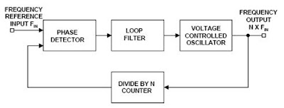
can be used as frequency multiplier. Figure3.1 shows how PLL works as frequency
multiplier.
Phase Locked Loop (PLL) circuits are
used for frequency control. They can be configured as frequency multipliers,
demodulators, tracking generators or clock recovery circuits. Each of these
applications demands different characteristics but they all use the same basic
circuit concept. Figure 3.1 contains a block diagram of a basic PLL frequency
multiplier. The operation of this circuit is typical of all phase locked loops.
It is basically a feedback control system that controls the phase of a voltage
controlled oscillator (VCO). The input signal is applied to one input of a
phase detector. The other input is connected to the output of a divide by N
counter. Normally the frequencies of both signals will be nearly the same. The
output of the phase detector is a voltage proportional to the phase difference
between the two inputs. This signal is applied to the loop filter. It is the
loop filter that determines the dynamic characteristics of the PLL. The
filtered signal controls the VCO. Note that the output of the VCO is at a frequency
that is N times the input supplied to the frequency reference input. This
output signal is sent back to the phase detector via the divide by N counter.
Normally the loop filter is designed to match the characteristics required by
the application of the PLL. If the PLL is to acquire and track a signal the
bandwidth of the loop filter will be greater than if it expects a fixed input
frequency. The frequency range which the PLL will accept and lock on is called
the capture range. Once the PLL is locked and tracking a signal the range of
frequencies that the PLL will follow is called the tracking range. Generally
the tracking range is larger than the capture range.
The
Xilinx Spartan-3 and VirtexIIPro series FPGA are all equipped with DCM (Digital
Clock Manager) modules which can precisely control the system clock [8]. There
are four DCMs available in spartan-3 kit which is considered as target device
for this project. There are three ways to use the DCM. First, calling DCM as a component is through HDL.
Second is through schematic i.e. taking as a symbol and assign ports for
required pins, then create user symbol to use in schematic. Third is through
XILINX clocking wizard from IP (Coregen & Architecture wizard). Third
one is the easiest way which is explained in subsection
Procedure
to Use DCM
Step1: Double-click Create New Source
– Select IP (COREGen & Architecture
Wizard), and click Next
The Architecture Wizard Contains Several Wizards as shown in figure 3.2.
Figure
3.2 Selecting a DCM from clocking wizard
Step2:
The Clocking Wizard helps you define the DCM. In main window
– Select pins
– Specify
• Reference source
• Clock frequency
• Phase shift
Figure 3.3 General setup wizard for DCM as a
frequency multiplier
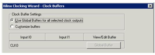
Step3: Specify the
Types of Clock Buffers
Connect clock
buffers (BUFG, BUFGMUX) to the selected output pins of the DCM
The DCM will appear in source window and ready to
use as a component. It can also be used in schematic by making it as a user
symbol through ‘design utilities’ option as shown in Figure3.5. Figure 3.6
shows behavioral simulation of DCM as frequency multiplier.
Figure 3.5 DCM used as a symbol in schematic design
entry
Figure
3.6 Behavioral simulation of frequency multiplier


No comments:
Post a Comment